A printed circuit board(PCB) is a board used to hold electronic part assembly by soldering them onto the board. PCBs are made up of various forms of insulating materials such as woven glass fabric reinforced by epoxide resin or polyimide forms and others. The electronics parts IC, resistors, capacitors are connected with copper tracks that are printed onto the PCB. The PCB can be produced with different architecture depending primarily upon the necessity of density of electronic component to be soldered to reduce cost.
Broadly we can classify PCB architecture into 3 categories or types as follows:
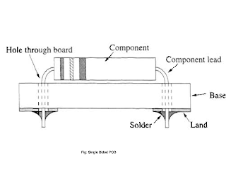
The picture below shows single sided PCB
In Single PCB, components are placed on one side of the board and the copper tracks are printed on the another side. The components are connected to the copper tracks via holes through the board.
2. Double Sided PCB
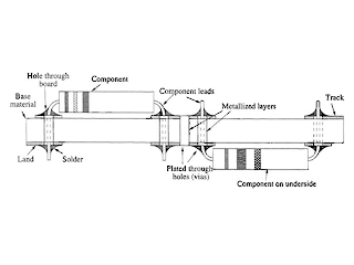
The picture below shows double sided PCB
In Double Sided PCB, components and copper tracks are found on both sides of the board. However usually, components are placed on one side and tracks on top and bottom are interconnected with plated through vias. With surface mounted components, they may also be placed on either side of the board and tracks are also printed on both sides of the board with interconnection between them using plated through vias.
3. Multilayer PCB
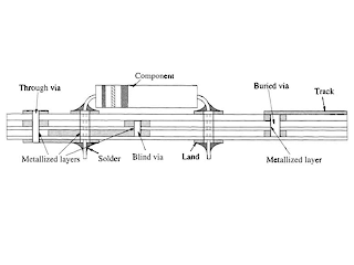
The picture below shows multilayer PCB
Multilayer PCB is one made up of more than 3 layers of insulating board. When top and bottom copper tracks are to be interconnected plated through vias are used. And when copper tracks inside the middle boards are to be connected either to the other middle layer board or top or bottom layer copper tracks then burried vias or blind vias are used.
Broadly we can classify PCB architecture into 3 categories or types as follows:
- Single Sided PCB
- Double Sided PCB
- Multilayer PCB
The picture below shows single sided PCB
 |
| Fig 1: Single Sided PCB |
2. Double Sided PCB
The picture below shows double sided PCB
 |
| Fig 2: Double Sided PCB |
3. Multilayer PCB
The picture below shows multilayer PCB
 |
| Fig 3: Multilayer PCB |
Tidak ada komentar:
Posting Komentar