Altium Designer has a very useful feature called the PCB Inspector. Using this PCB inspector one can quickly manipulate and gain insight to different components on the PCB board.
Often times during the component placement phase designer want to look at what various and possible ways there are to place the component(s). In such case the PCB inspector tool of Altium Designer is helpful.
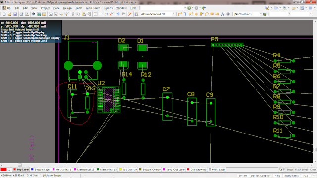
As an example it can be used to move components or parts between different layers and see how the component placement on other layer will have effect on the routing and overall design. To see this, consider the following PCB board with components on it.
Notice the capacitor C11 and resistor R13. This is a 2 layer PCB board. Suppose that we want to move these component to the other side and see how the track route and overall design will look like.
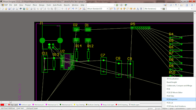
To do this, we select the PCB>PCB Inspector as shown-
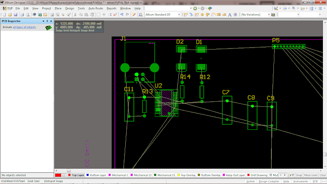
This will open the PCB Inspector panel-
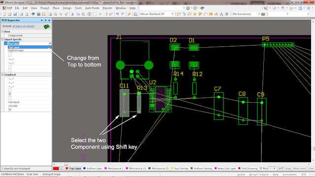
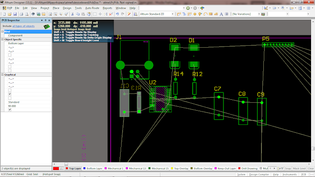
Now select the two components C11 and R13 by holding the shift key and the PCB Inspector will show properties and information of the selected components. Now change the layer from Top to bottom as shown below-
Now the component are placed in the bottom layer as shown-
Now we can see how while placing the components down in the bottom layers the track routing has changed and the overall look of the design.
For more tutorials visit Altium Designer Tutorials
Tidak ada komentar:
Posting Komentar