This is a tutorial that shows how to create schematic symbol and footprint of the female N right angle bulkedge connector in altium designer. Specifically, an integrated library is created for the N connector is created using the datasheet from the manufacturer.
The N connector or Type N is widely used RF connector used to join the transceiver to the antenna using coaxial cable. It can be used for frequencies from DC to 18GHz and both 50ohm and 75ohm impedance is available. The Female N right angle bulkhead which can be mounted onto a PCB board is shown below-
The N connector used here is from the Pasternack and the model name is PE44398. The dimension of this connector is as shown-
This is a PCB mount type female N connector. It has 4 mounting hole and a center RF connector. The diameter of the mounting hole and the RF connector is 62mil. The mounting holes are separated by 400 mils.
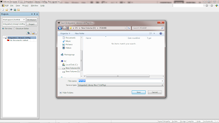
To create an integrated library for this connector, go to File>New>Project>Integrated Library. Once done a new library package with name Integrated_Library1.LibPkg will be created. It good practice to save and rename the newly created library with some identifying name. The model name of this connector is PE44398 so here the integrated library project is saved by right clicking and selecting Save Project As and save it with name PE44398 in some folder.
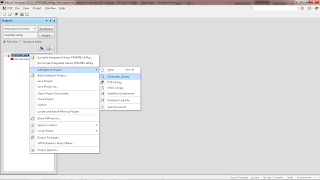
To create the schematic symbol and footprint for this part we have to add a schematic library and a PCB library. To add the schematic library, right click on the PE44398.PkgLib then select Add New to Project>Schematic Library. This is as shown-
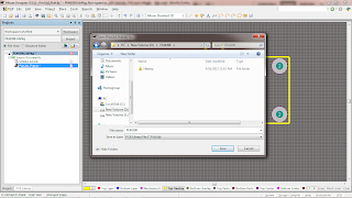
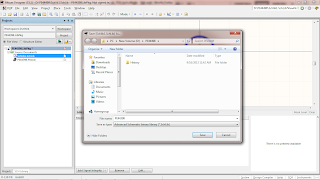
To save the schematic library with some name,
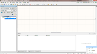
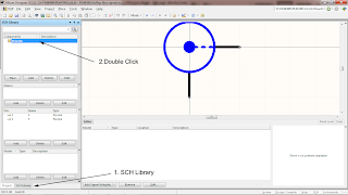
Now we have to create a schematic symbol for this N connector. We will here simply copy the BNC connector symbol and use it for N connector. To do this, go to SCH in the bottom right corner and select SCH library as shown-
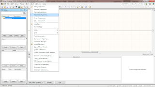
The schematic library with component_1 will be shown on the right hand side panel. To rename this component_1, go to Tool>Rename Component and give it some name such as "PE44398".
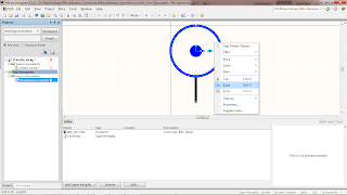
Now open the BNC connector schematic symbol and copy the symbol as shown-
Go back to the schematic library editor for the PE44398 and paste the copied symbol into the editor as shown below-
Next we have to create the footprint and then combine the footprint to the earlier created schematic symbol.
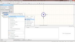
Now to create the footprint, go back to the integrated library project panel, select and right click the PE44398.PkgLib and select Add New to Library>PCB Library as shown-
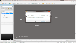
Here the footprint of the Female N right angle bulkhead will be designed. Click on the PCB Library tab visible in the left buttom(as shown in figure) and double click on the PCBCOMPONENT_1. This brings up a dialog box where you can specify the name for the pcb footprint part, provide height information and small description. Give it a name like PE44398, height of 990mils(see dimension diagram) and give a description "Female N Right Angle Bulkhead Connector" as shown-
Now we will draw the footprint for this N connector.
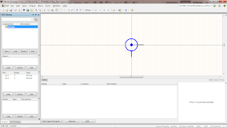
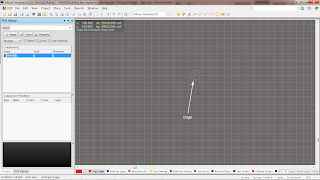
Notice the origin shown as a circle with cross-
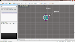
Now to draw the mechanical mounting part, click on the Place Pad icon in the top toolbar. A pad will attached to the cursor. Bring it to the origin and press the tab key
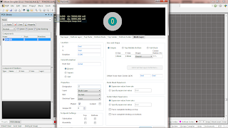
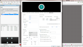
This will bring up a dialog box where we can enter the value for mounting drill hole and the pad size. Enter 62mils for the hole size, 130mils (X and Y) for the pad diameter and designator as 2(designator 1 will be used for the RF connector pin later on). Refer to the datasheet/diagram of the part provided above. This is shown below-
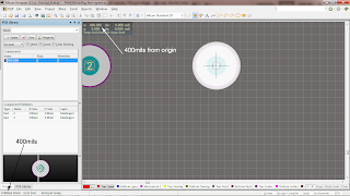
As soon as the pad is placed at the origin, a new pad will be attached to cursor. The new pad has to be placed 400mils to the right from the origin. Also press tab key and change the designator to 2(all mounting pad has designator 2). Go to the right by 400 mils and place the second mounting pad as shown-
As this second pad is placed another pad will be attached to the cursor, press tab key again and assign 2 as designator, go 400 mils vertically up and place it there. Similarly for the last fourth mounting pad repeat the process. After placing the 4 mounting pads the footprint will be like the one below-
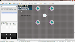
Now the RF connector pin pad and mounting hole will be placed. To do this click again on the Place Pad icon, and enter the pad information. Hole size should be 62mils, pad size(X and Y) should be 90 mils, designator is 1 and placed at the center of the 4 mounting pad(refer to the part diagram). The coordinate of this pin is (200mils, 200mils).
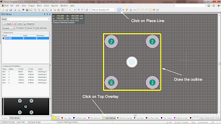
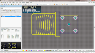
To draw the outline of the part, click on Top Overlay at the bottom, then select Place Line icon and draw the rectangular outline around the pads as shown-
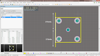
Select the line tool again, go to the middle of the left line and press insert key to make it the temporary origin as shown-
From the temporary origin draw a line vertically upwards and downwards of 375mils.
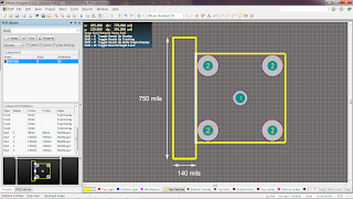
Now starting from any of the tip of the new line draw a rectangle with width of 140 mils as shown-
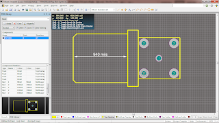
Similarly draw the following rectangle with the provided dimension-
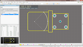
Select the Place by Arc Edge icon and draw an arc like the one as shown-
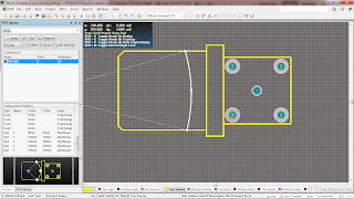
Drag the arc from the arc end to make it more sharp like the one shown below-
Now copy and paste the arc several times as shown-
Now we have completed the footprint for the part.
Go to the project panel again, right click on the PCB library part and select Save As to save the pcb library part with some name "PE44398" as shown-
Similarly save the Schlib1.SchLib with some name such as PE44398.Schlib as shown-
Now to give the schematic part some designator, description and add footprint information, click on the SCH Library and then double click on the PE44398 part as shown-
This brings up the dialog box to provide information for the schematic component. For default designator type J? , provide some default comment such as N Plug Connector, provide description- Female N Right Angle Bulkedge Connector.
Then click on the Add>Footprint which is visible at the bottom of the screen of the dialog box as shown-
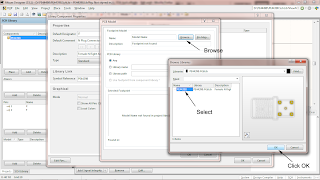
When the add footprint is selected, a dialog box will appear that allows us to attach the footprint. Click on the browse button, then select the footprint and click OK to attach the footprint as shown below-
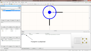
Now the footprint is attached-
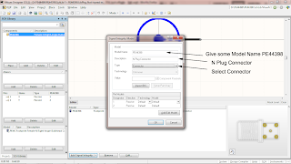
To add the Signal Integrity information, click on the Add Signal Integrity. In the dialog box that appears, give some model name for eg. PE44398, description- N Plug connector and select Type as Connector as shown-
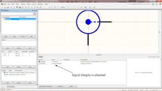
The Signal Integrity is also attached now-
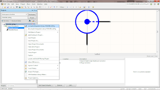
To complete the creation of the part as an integrated library part, go back to the project panel, select the PE44398.LibPkg, right click and select Compile Integrated Library PE44398.LibPkg to compile the integrated library project as shown
Now the new N connector part is created with integrated library that has all information- schematic, footprint and signal integrity. This part is now ready to be used.
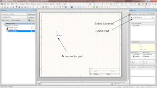
As an example, open a new schematic sheet and browse to the library, select the PE44398.IntLib then select the part and place it on the schematic as shown-





Pcb Mount N Connector Schematic, Footprint Creation Tutorial >>>>> Download Now
BalasHapus>>>>> Download Full
Pcb Mount N Connector Schematic, Footprint Creation Tutorial >>>>> Download LINK
>>>>> Download Now
Pcb Mount N Connector Schematic, Footprint Creation Tutorial >>>>> Download Full
>>>>> Download LINK 3T