In this communication system project using Proteus 8 software a simple communication system is shown using two PIC16F84A microcontrollers which acts as a transmitter and receiver. Assembly code for the two microcontroller is provided and shown how these microcontroller communicate.
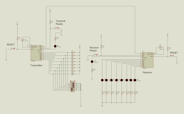
The basic communication is via a simple protocol which allows the two micro-controllers to communicate. The switches at the transmitter MC are used as input and converted to message and sent to the receiving microcontroller serially. The received message is then shown to light up the output leds at the receiver. In other words the state of the switches forms the message to be sent and the LED glow at the receiver forms the message received.
The Schematic for this communication system is shown below-
The components used are-
To generate the hex code open the MpLAB and create a new project by clicking on the Project>Project Wizard.
A new window will pop-up, click next. Then in the next window select PIC16F84A, then click next. In the language toolsuite option, select Microchip MPASM Toolsuite as shown-
In the next window step 3, select a folder where you want to save the project and the name of the project.
Then the step 4 allows you to add files to the project. Add the following files-
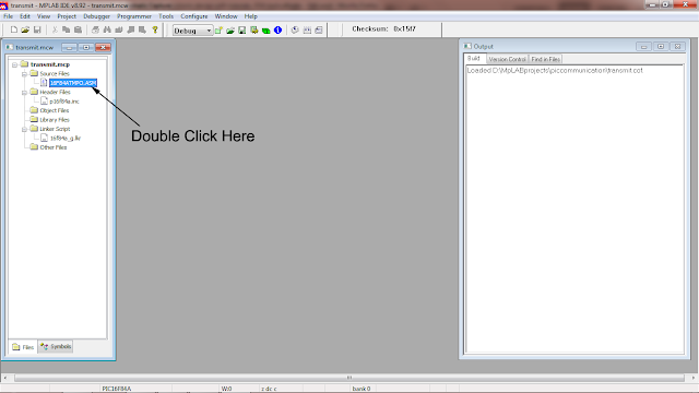
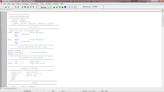
For the transmitter microcontroller, open the 16F84ATEMO.asm template just created by double clicking on it and copy-paste the below assembly code for the transmitter.
Transmitter Microcontroller Source Code:
;=========================
; setup and configuration
;=========================
processor 16f84A
include <p16f84A.inc>
__config _XT_OSC & _WDT_OFF & _PWRTE_ON & _CP_OFF
;============================================================
; M A C R O S
;============================================================
; Macros to select the register banks
Bank0 MACRO ; Select RAM bank 0
bcf STATUS,RP0
ENDM
Bank1 MACRO ; Select RAM bank 1
bsf STATUS,RP0
ENDM
;=====================================================
; constant definitions for pin wiring
;=====================================================
#define readySW 2 ;|
#define readyLED 3 ;| -- from wiring diagram
#define serialLN 0 ;|
;=====================================================
; PIC register and flag equates
;=====================================================
c equ 0 ; Carry flag
tmrOVF equ 2 ; Timer overflow bit
;
;======================================================
; variables in PIC RAM
;=====================================================
cblock 0x0c ; Start of block
bitCount ; Counter for 8 bits
rcvReg ; Data to send
temp
endc
;=========================================================
; program
;=========================================================
org 0 ; start at address
goto main
; Space for interrupt handlers
org 0x04
main:
Bank1
; Port A bits 0 and 2 are input. All others are output
movlw b'00000101' ; port A setup
movwf TRISA
; Port B is all output
movlw b'00000000' ; port B setup
MOVWF TRISB
Bank0
; Turn off all port B LEDs
clrf PORTB
; And receiver register
clrf rcvReg
; Prepare to set prescaler
clrf TMR0
clrwdt
; Setup OPTION register for full timer speed
movlw b'11011000'
; 1 1 0 1 1 0 0 0 <= OPTION bits
; | | | | | |__|__|_____ PS2-PS0 (prescaler bits)
; | | | | | Values for Timer0
; | | | | | *000 = 1:2 001 = 1:4
; | | | | | 010 = 1:8 011 = 1:16
; | | | | | 100 = 1:32 101 = 1:64
; | | | | | 110 = 1:128 111 = 1:256
; | | | | |______________ PSA (prescaler assign)
; | | | | *1 = to WDT
; | | | | 0 = to Timer0
; | | | |_________________ TOSE (Timer0 edge select)
; | | | 0 = increment on low-to-high
; | | | *1 = increment in high-to-low
; | | |____________________ TOCS (TMR0 clock source)
; | | *0 = internal clock
; | | 1 = RA4/TOCKI bit source
; | |_______________________ INTEDG (Edge select)
; | 0 = falling edge
; | *1 = raising edge
; |__________________________ RBPU pullups
; 0 = enabled
; *1 = dissabled
option
; Dissable interrupts
bcf INTCON,5 ; Timer0 overflow dissabled
bcf INTCON,7 ; Global interupts dissabled
;=========================
; wait for READY switch
; to be pressed
;=========================
ready2rcv:
btfsc PORTA,readySW ; Test switch
goto ready2rcv ; loop
; Turn ON the ready-to-receive LED
bsf PORTA,readyLED
;===========================
; receiving
;===========================
call rcvData ; Call serial input procedure
;===========================
; data received
;===========================
; Turn ready to receive LED off
bcf PORTA,readyLED
; Display received data
movf rcvReg,w ; Byte received to w
movwf PORTB ; display in port B
;===========================
; wait forever
;===========================
endloop:
goto endloop
;============================================================
; procedure to receive serial data
;============================================================
; ON ENTRY:
; local variable dataReg is used to store 8-bit value
; received through port (labeled serialLN)
; OPERATION:
; 1. The timer at register TMR0 is set to run at
; maximum clock speed, that is, 256 clock beats.
; The timer overflow flag in the INTCON register
; is set when the timer cycles from 0xff to 0x00.
; 2. When the START signal is received, the code
; waits for 128 timer beats so as to read data in
; the middle of the send period.
; 3. Each bit (start, data, and stop bits) is read
; at intervals of 256 timer beats.
; 4. The procedure tests the timer ofverflow flag
; (tmrOVF) to determine when the timer cycle has
; ended, that is when 256 clock beats have passed.
;------------------------------------------------------------
rcvData:
clrf TMR0 ; Reset timer
movlw 0x08 ; Initialize bit counter
movwf bitCount
;=========================
; wait for START bit
;=========================
startWait:
btfsc PORTA,0 ; Is port A0 low?
goto startWait ; No. Wait for mark
;=========================
; offset 128 clock beats
;=========================
; At this point the receiver has found the falling
; edge of the start bit. It must now wait 128 timer
; beats to synchronize in the middle of the sender's
; data rate, as follows:
; |<========= falling edge of START bit
; |
; |-----|<====== 128 clock beats offset
; ----------. | .---------
; | | <== SIGNAL
; -----------
; |<-- 256 -->|
;
movlw 0x80 ; 128 clock beats offset
movwf TMR0 ; to TMR0 counter
bcf INTCON,tmrOVF ; Clear overflow flag
offsetWait:
btfss INTCON,tmrOVF ; timer overflow?
goto offsetWait ; wait until
btfsc PORTA,0 ; Test start bit for error
goto offsetWait ; Recycle if a false start
;==========================
; receive data
;==========================
clrf TMR0 ; Restart timer
bcf INTCON,tmrOVF ; Clear overflow flag
; Wait for 256 timer cycles for first/next data bit
bitWait:
btfss INTCON,tmrOVF ; Timer cycle end?
goto bitWait ; Keep waiting
; Timer has counter 256 beats
bcf INTCON,tmrOVF ; Reset overflow flag
movf PORTA,w ; Read port A into w
movwf temp ; Store value read
rrf temp,f ; Rotate bit 0 into carry flag
rlf rcvReg,f ; Rotate carry into rcvReg bit 0
decfsz bitCount,f ; 8 bits received
goto bitWait ; Next bit
; Wait for one time cycle at end of reception
markWait:
btfss INTCON,tmrOVF ; timer overflow flag
goto markWait ; keep waiting
;========================
; end of reception
;========================
return
;=========================================================
; end of program
;=========================================================
end
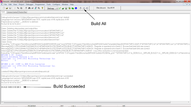
Once copied click on Build All option to start compiling the assembly code. Once this is complete, it should show Build Succeeded as shown below-
This create a transmit.hex (transmit is the project name here) in the MpLAB project folder. See below-
Copy the transmit.hex file into your microcontroller proteus project folder. See example below-
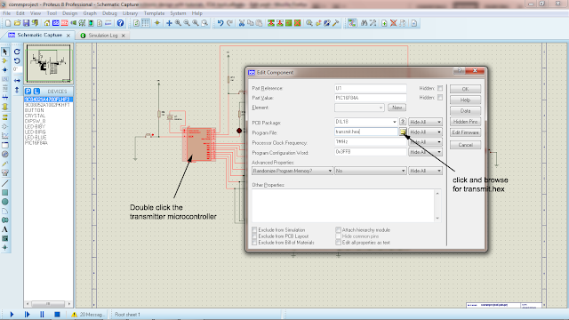
Now to burn the transmit.hex file to the transmitter microcontroller, go to the schematic and double click on the transmitter microcontroller to bring up its properties window. Then click on the folder icon and browse for the transmit.hex file and click ok to exit the window.
Now the transmitter microcontroller is ready for simulation.
Repeat the same steps for the receiver microcontroller by starting by creating a new MpLAB project, adding the same files, copying and pasting the receiver assembly code provided below, compiling and creating a receive.hex file and lastly uploading the hex file to the receiver microcontroller.
Receiver Microcontroller Source Code:
;=========================
; setup and configuration
;=========================
processor 16f84A
include <p16f84A.inc>
__config _XT_OSC & _WDT_OFF & _PWRTE_ON & _CP_OFF
;============================================================
; M A C R O S
;============================================================
; Macros to select the register banks
Bank0 MACRO ; Select RAM bank 0
bcf STATUS,RP0
ENDM
Bank1 MACRO ; Select RAM bank 1
bsf STATUS,RP0
ENDM
;=====================================================
; constant definitions for pin wiring
;=====================================================
#define readySW 2 ;|
#define readyLED 3 ;| -- from wiring diagram
#define serialLN 0 ;|
;=====================================================
; PIC register and flag equates
;=====================================================
c equ 0 ; Carry flag
tmrOVF equ 2 ; Timer overflow bit
;
;======================================================
; variables in PIC RAM
;=====================================================
cblock 0x0c ; Start of block
bitCount ; Counter for 8 bits
rcvReg ; Data to send
temp
endc
;=========================================================
; program
;=========================================================
org 0 ; start at address
goto main
; Space for interrupt handlers
org 0x04
main:
Bank1
; Port A bits 0 and 2 are input. All others are output
movlw b'00000101' ; port A setup
movwf TRISA
; Port B is all output
movlw b'00000000' ; port B setup
MOVWF TRISB
Bank0
; Turn off all port B LEDs
clrf PORTB
; And receiver register
clrf rcvReg
; Prepare to set prescaler
clrf TMR0
clrwdt
; Setup OPTION register for full timer speed
movlw b'11011000'
; 1 1 0 1 1 0 0 0 <= OPTION bits
; | | | | | |__|__|_____ PS2-PS0 (prescaler bits)
; | | | | | Values for Timer0
; | | | | | *000 = 1:2 001 = 1:4
; | | | | | 010 = 1:8 011 = 1:16
; | | | | | 100 = 1:32 101 = 1:64
; | | | | | 110 = 1:128 111 = 1:256
; | | | | |______________ PSA (prescaler assign)
; | | | | *1 = to WDT
; | | | | 0 = to Timer0
; | | | |_________________ TOSE (Timer0 edge select)
; | | | 0 = increment on low-to-high
; | | | *1 = increment in high-to-low
; | | |____________________ TOCS (TMR0 clock source)
; | | *0 = internal clock
; | | 1 = RA4/TOCKI bit source
; | |_______________________ INTEDG (Edge select)
; | 0 = falling edge
; | *1 = raising edge
; |__________________________ RBPU pullups
; 0 = enabled
; *1 = dissabled
option
; Dissable interrupts
bcf INTCON,5 ; Timer0 overflow dissabled
bcf INTCON,7 ; Global interupts dissabled
;=========================
; wait for READY switch
; to be pressed
;=========================
ready2rcv:
btfsc PORTA,readySW ; Test switch
goto ready2rcv ; loop
; Turn ON the ready-to-receive LED
bsf PORTA,readyLED
;===========================
; receiving
;===========================
call rcvData ; Call serial input procedure
;===========================
; data received
;===========================
; Turn ready to receive LED off
bcf PORTA,readyLED
; Display received data
movf rcvReg,w ; Byte received to w
movwf PORTB ; display in port B
;===========================
; wait forever
;===========================
endloop:
goto endloop
;============================================================
; procedure to receive serial data
;============================================================
; ON ENTRY:
; local variable dataReg is used to store 8-bit value
; received through port (labeled serialLN)
; OPERATION:
; 1. The timer at register TMR0 is set to run at
; maximum clock speed, that is, 256 clock beats.
; The timer overflow flag in the INTCON register
; is set when the timer cycles from 0xff to 0x00.
; 2. When the START signal is received, the code
; waits for 128 timer beats so as to read data in
; the middle of the send period.
; 3. Each bit (start, data, and stop bits) is read
; at intervals of 256 timer beats.
; 4. The procedure tests the timer ofverflow flag
; (tmrOVF) to determine when the timer cycle has
; ended, that is when 256 clock beats have passed.
;------------------------------------------------------------
rcvData:
clrf TMR0 ; Reset timer
movlw 0x08 ; Initialize bit counter
movwf bitCount
;=========================
; wait for START bit
;=========================
startWait:
btfsc PORTA,0 ; Is port A0 low?
goto startWait ; No. Wait for mark
;=========================
; offset 128 clock beats
;=========================
; At this point the receiver has found the falling
; edge of the start bit. It must now wait 128 timer
; beats to synchronize in the middle of the sender's
; data rate, as follows:
; |<========= falling edge of START bit
; |
; |-----|<====== 128 clock beats offset
; ----------. | .---------
; | | <== SIGNAL
; -----------
; |<-- 256 -->|
;
movlw 0x80 ; 128 clock beats offset
movwf TMR0 ; to TMR0 counter
bcf INTCON,tmrOVF ; Clear overflow flag
offsetWait:
btfss INTCON,tmrOVF ; timer overflow?
goto offsetWait ; wait until
btfsc PORTA,0 ; Test start bit for error
goto offsetWait ; Recycle if a false start
;==========================
; receive data
;==========================
clrf TMR0 ; Restart timer
bcf INTCON,tmrOVF ; Clear overflow flag
; Wait for 256 timer cycles for first/next data bit
bitWait:
btfss INTCON,tmrOVF ; Timer cycle end?
goto bitWait ; Keep waiting
; Timer has counter 256 beats
bcf INTCON,tmrOVF ; Reset overflow flag
movf PORTA,w ; Read port A into w
movwf temp ; Store value read
rrf temp,f ; Rotate bit 0 into carry flag
rlf rcvReg,f ; Rotate carry into rcvReg bit 0
decfsz bitCount,f ; 8 bits received
goto bitWait ; Next bit
; Wait for one time cycle at end of reception
markWait:
btfss INTCON,tmrOVF ; timer overflow flag
goto markWait ; keep waiting
;========================
; end of reception
;========================
return
;=========================================================
; end of program
;=========================================================
end
The basic communication is via a simple protocol which allows the two micro-controllers to communicate. The switches at the transmitter MC are used as input and converted to message and sent to the receiving microcontroller serially. The received message is then shown to light up the output leds at the receiver. In other words the state of the switches forms the message to be sent and the LED glow at the receiver forms the message received.
The Schematic for this communication system is shown below-
The components used are-
- 9C04021A4700FLHF3(470 ohm resistor)
- 9C08052A1002FKHFT(10k ohm resistor)
- Button
- Crystal
- DIPSW_8
- LED-BIBY
- LED-BIBG
- LED-BLUE
- PIC16F84A(micro-controller)
To generate the hex code open the MpLAB and create a new project by clicking on the Project>Project Wizard.
A new window will pop-up, click next. Then in the next window select PIC16F84A, then click next. In the language toolsuite option, select Microchip MPASM Toolsuite as shown-
In the next window step 3, select a folder where you want to save the project and the name of the project.
Then the step 4 allows you to add files to the project. Add the following files-
- C:\Program Files\Microchip\MPASM Suite\LKR\16f84a_g.lkr
- C:\Program Files\Microchip\MPASM Suite\p16f84a.inc
- C:\Program Files\Microchip\MPASM Suite\Template\Object\16F84ATEMO.ASM
For the transmitter microcontroller, open the 16F84ATEMO.asm template just created by double clicking on it and copy-paste the below assembly code for the transmitter.
Transmitter Microcontroller Source Code:
;=========================
; setup and configuration
;=========================
processor 16f84A
include <p16f84A.inc>
__config _XT_OSC & _WDT_OFF & _PWRTE_ON & _CP_OFF
;============================================================
; M A C R O S
;============================================================
; Macros to select the register banks
Bank0 MACRO ; Select RAM bank 0
bcf STATUS,RP0
ENDM
Bank1 MACRO ; Select RAM bank 1
bsf STATUS,RP0
ENDM
;=====================================================
; constant definitions for pin wiring
;=====================================================
#define readySW 2 ;|
#define readyLED 3 ;| -- from wiring diagram
#define serialLN 0 ;|
;=====================================================
; PIC register and flag equates
;=====================================================
c equ 0 ; Carry flag
tmrOVF equ 2 ; Timer overflow bit
;
;======================================================
; variables in PIC RAM
;=====================================================
cblock 0x0c ; Start of block
bitCount ; Counter for 8 bits
rcvReg ; Data to send
temp
endc
;=========================================================
; program
;=========================================================
org 0 ; start at address
goto main
; Space for interrupt handlers
org 0x04
main:
Bank1
; Port A bits 0 and 2 are input. All others are output
movlw b'00000101' ; port A setup
movwf TRISA
; Port B is all output
movlw b'00000000' ; port B setup
MOVWF TRISB
Bank0
; Turn off all port B LEDs
clrf PORTB
; And receiver register
clrf rcvReg
; Prepare to set prescaler
clrf TMR0
clrwdt
; Setup OPTION register for full timer speed
movlw b'11011000'
; 1 1 0 1 1 0 0 0 <= OPTION bits
; | | | | | |__|__|_____ PS2-PS0 (prescaler bits)
; | | | | | Values for Timer0
; | | | | | *000 = 1:2 001 = 1:4
; | | | | | 010 = 1:8 011 = 1:16
; | | | | | 100 = 1:32 101 = 1:64
; | | | | | 110 = 1:128 111 = 1:256
; | | | | |______________ PSA (prescaler assign)
; | | | | *1 = to WDT
; | | | | 0 = to Timer0
; | | | |_________________ TOSE (Timer0 edge select)
; | | | 0 = increment on low-to-high
; | | | *1 = increment in high-to-low
; | | |____________________ TOCS (TMR0 clock source)
; | | *0 = internal clock
; | | 1 = RA4/TOCKI bit source
; | |_______________________ INTEDG (Edge select)
; | 0 = falling edge
; | *1 = raising edge
; |__________________________ RBPU pullups
; 0 = enabled
; *1 = dissabled
option
; Dissable interrupts
bcf INTCON,5 ; Timer0 overflow dissabled
bcf INTCON,7 ; Global interupts dissabled
;=========================
; wait for READY switch
; to be pressed
;=========================
ready2rcv:
btfsc PORTA,readySW ; Test switch
goto ready2rcv ; loop
; Turn ON the ready-to-receive LED
bsf PORTA,readyLED
;===========================
; receiving
;===========================
call rcvData ; Call serial input procedure
;===========================
; data received
;===========================
; Turn ready to receive LED off
bcf PORTA,readyLED
; Display received data
movf rcvReg,w ; Byte received to w
movwf PORTB ; display in port B
;===========================
; wait forever
;===========================
endloop:
goto endloop
;============================================================
; procedure to receive serial data
;============================================================
; ON ENTRY:
; local variable dataReg is used to store 8-bit value
; received through port (labeled serialLN)
; OPERATION:
; 1. The timer at register TMR0 is set to run at
; maximum clock speed, that is, 256 clock beats.
; The timer overflow flag in the INTCON register
; is set when the timer cycles from 0xff to 0x00.
; 2. When the START signal is received, the code
; waits for 128 timer beats so as to read data in
; the middle of the send period.
; 3. Each bit (start, data, and stop bits) is read
; at intervals of 256 timer beats.
; 4. The procedure tests the timer ofverflow flag
; (tmrOVF) to determine when the timer cycle has
; ended, that is when 256 clock beats have passed.
;------------------------------------------------------------
rcvData:
clrf TMR0 ; Reset timer
movlw 0x08 ; Initialize bit counter
movwf bitCount
;=========================
; wait for START bit
;=========================
startWait:
btfsc PORTA,0 ; Is port A0 low?
goto startWait ; No. Wait for mark
;=========================
; offset 128 clock beats
;=========================
; At this point the receiver has found the falling
; edge of the start bit. It must now wait 128 timer
; beats to synchronize in the middle of the sender's
; data rate, as follows:
; |<========= falling edge of START bit
; |
; |-----|<====== 128 clock beats offset
; ----------. | .---------
; | | <== SIGNAL
; -----------
; |<-- 256 -->|
;
movlw 0x80 ; 128 clock beats offset
movwf TMR0 ; to TMR0 counter
bcf INTCON,tmrOVF ; Clear overflow flag
offsetWait:
btfss INTCON,tmrOVF ; timer overflow?
goto offsetWait ; wait until
btfsc PORTA,0 ; Test start bit for error
goto offsetWait ; Recycle if a false start
;==========================
; receive data
;==========================
clrf TMR0 ; Restart timer
bcf INTCON,tmrOVF ; Clear overflow flag
; Wait for 256 timer cycles for first/next data bit
bitWait:
btfss INTCON,tmrOVF ; Timer cycle end?
goto bitWait ; Keep waiting
; Timer has counter 256 beats
bcf INTCON,tmrOVF ; Reset overflow flag
movf PORTA,w ; Read port A into w
movwf temp ; Store value read
rrf temp,f ; Rotate bit 0 into carry flag
rlf rcvReg,f ; Rotate carry into rcvReg bit 0
decfsz bitCount,f ; 8 bits received
goto bitWait ; Next bit
; Wait for one time cycle at end of reception
markWait:
btfss INTCON,tmrOVF ; timer overflow flag
goto markWait ; keep waiting
;========================
; end of reception
;========================
return
;=========================================================
; end of program
;=========================================================
end
Once copied click on Build All option to start compiling the assembly code. Once this is complete, it should show Build Succeeded as shown below-
This create a transmit.hex (transmit is the project name here) in the MpLAB project folder. See below-
Copy the transmit.hex file into your microcontroller proteus project folder. See example below-
Now to burn the transmit.hex file to the transmitter microcontroller, go to the schematic and double click on the transmitter microcontroller to bring up its properties window. Then click on the folder icon and browse for the transmit.hex file and click ok to exit the window.
Now the transmitter microcontroller is ready for simulation.
Repeat the same steps for the receiver microcontroller by starting by creating a new MpLAB project, adding the same files, copying and pasting the receiver assembly code provided below, compiling and creating a receive.hex file and lastly uploading the hex file to the receiver microcontroller.
Receiver Microcontroller Source Code:
;=========================
; setup and configuration
;=========================
processor 16f84A
include <p16f84A.inc>
__config _XT_OSC & _WDT_OFF & _PWRTE_ON & _CP_OFF
;============================================================
; M A C R O S
;============================================================
; Macros to select the register banks
Bank0 MACRO ; Select RAM bank 0
bcf STATUS,RP0
ENDM
Bank1 MACRO ; Select RAM bank 1
bsf STATUS,RP0
ENDM
;=====================================================
; constant definitions for pin wiring
;=====================================================
#define readySW 2 ;|
#define readyLED 3 ;| -- from wiring diagram
#define serialLN 0 ;|
;=====================================================
; PIC register and flag equates
;=====================================================
c equ 0 ; Carry flag
tmrOVF equ 2 ; Timer overflow bit
;
;======================================================
; variables in PIC RAM
;=====================================================
cblock 0x0c ; Start of block
bitCount ; Counter for 8 bits
rcvReg ; Data to send
temp
endc
;=========================================================
; program
;=========================================================
org 0 ; start at address
goto main
; Space for interrupt handlers
org 0x04
main:
Bank1
; Port A bits 0 and 2 are input. All others are output
movlw b'00000101' ; port A setup
movwf TRISA
; Port B is all output
movlw b'00000000' ; port B setup
MOVWF TRISB
Bank0
; Turn off all port B LEDs
clrf PORTB
; And receiver register
clrf rcvReg
; Prepare to set prescaler
clrf TMR0
clrwdt
; Setup OPTION register for full timer speed
movlw b'11011000'
; 1 1 0 1 1 0 0 0 <= OPTION bits
; | | | | | |__|__|_____ PS2-PS0 (prescaler bits)
; | | | | | Values for Timer0
; | | | | | *000 = 1:2 001 = 1:4
; | | | | | 010 = 1:8 011 = 1:16
; | | | | | 100 = 1:32 101 = 1:64
; | | | | | 110 = 1:128 111 = 1:256
; | | | | |______________ PSA (prescaler assign)
; | | | | *1 = to WDT
; | | | | 0 = to Timer0
; | | | |_________________ TOSE (Timer0 edge select)
; | | | 0 = increment on low-to-high
; | | | *1 = increment in high-to-low
; | | |____________________ TOCS (TMR0 clock source)
; | | *0 = internal clock
; | | 1 = RA4/TOCKI bit source
; | |_______________________ INTEDG (Edge select)
; | 0 = falling edge
; | *1 = raising edge
; |__________________________ RBPU pullups
; 0 = enabled
; *1 = dissabled
option
; Dissable interrupts
bcf INTCON,5 ; Timer0 overflow dissabled
bcf INTCON,7 ; Global interupts dissabled
;=========================
; wait for READY switch
; to be pressed
;=========================
ready2rcv:
btfsc PORTA,readySW ; Test switch
goto ready2rcv ; loop
; Turn ON the ready-to-receive LED
bsf PORTA,readyLED
;===========================
; receiving
;===========================
call rcvData ; Call serial input procedure
;===========================
; data received
;===========================
; Turn ready to receive LED off
bcf PORTA,readyLED
; Display received data
movf rcvReg,w ; Byte received to w
movwf PORTB ; display in port B
;===========================
; wait forever
;===========================
endloop:
goto endloop
;============================================================
; procedure to receive serial data
;============================================================
; ON ENTRY:
; local variable dataReg is used to store 8-bit value
; received through port (labeled serialLN)
; OPERATION:
; 1. The timer at register TMR0 is set to run at
; maximum clock speed, that is, 256 clock beats.
; The timer overflow flag in the INTCON register
; is set when the timer cycles from 0xff to 0x00.
; 2. When the START signal is received, the code
; waits for 128 timer beats so as to read data in
; the middle of the send period.
; 3. Each bit (start, data, and stop bits) is read
; at intervals of 256 timer beats.
; 4. The procedure tests the timer ofverflow flag
; (tmrOVF) to determine when the timer cycle has
; ended, that is when 256 clock beats have passed.
;------------------------------------------------------------
rcvData:
clrf TMR0 ; Reset timer
movlw 0x08 ; Initialize bit counter
movwf bitCount
;=========================
; wait for START bit
;=========================
startWait:
btfsc PORTA,0 ; Is port A0 low?
goto startWait ; No. Wait for mark
;=========================
; offset 128 clock beats
;=========================
; At this point the receiver has found the falling
; edge of the start bit. It must now wait 128 timer
; beats to synchronize in the middle of the sender's
; data rate, as follows:
; |<========= falling edge of START bit
; |
; |-----|<====== 128 clock beats offset
; ----------. | .---------
; | | <== SIGNAL
; -----------
; |<-- 256 -->|
;
movlw 0x80 ; 128 clock beats offset
movwf TMR0 ; to TMR0 counter
bcf INTCON,tmrOVF ; Clear overflow flag
offsetWait:
btfss INTCON,tmrOVF ; timer overflow?
goto offsetWait ; wait until
btfsc PORTA,0 ; Test start bit for error
goto offsetWait ; Recycle if a false start
;==========================
; receive data
;==========================
clrf TMR0 ; Restart timer
bcf INTCON,tmrOVF ; Clear overflow flag
; Wait for 256 timer cycles for first/next data bit
bitWait:
btfss INTCON,tmrOVF ; Timer cycle end?
goto bitWait ; Keep waiting
; Timer has counter 256 beats
bcf INTCON,tmrOVF ; Reset overflow flag
movf PORTA,w ; Read port A into w
movwf temp ; Store value read
rrf temp,f ; Rotate bit 0 into carry flag
rlf rcvReg,f ; Rotate carry into rcvReg bit 0
decfsz bitCount,f ; 8 bits received
goto bitWait ; Next bit
; Wait for one time cycle at end of reception
markWait:
btfss INTCON,tmrOVF ; timer overflow flag
goto markWait ; keep waiting
;========================
; end of reception
;========================
return
;=========================================================
; end of program
;=========================================================
end




Tidak ada komentar:
Posting Komentar