ASK modulation is digital modulation technique wherein binary message signal stream is impressed onto the high frequency carrier signal for transmission over larger bandwidth channels such as air. The binary message signal stream is of unipolar type, that means that 1V represents logical 1 and 0V represents the logical 0 bit. The binary message stream turns On/Off the modulator such that the high frequency carrier signal is transmitted when modulator is switched on and during the off state nothing is transmitted.
In orcad capture a voltage controlled switch called Sbreak can be used to stimulate the behavior of the modulator. In reality a modulator is made of transistors that switches on/off in response to clock impulses supplied to it.
The schematic for simulating ASK modulation is shown in figure below-
In the schematic, the message signal labelled Message_Signal is a binary unipolar signal with V1=0V and V2=1V, TD=0s, TR=0.01us, TF=0.01us, PW=30us and PER=90us. The carrier signal labelled Carrier_Signal is a sinusoid with amplitude VAMPL=10V and frequency of 100KHz. The message binary sequence turns on/off the switch and carrier signal is transmitted as ASK signal labelled ASK_Signal. The 1k load resistance at the output simulates the resistance of the switch(modulator).
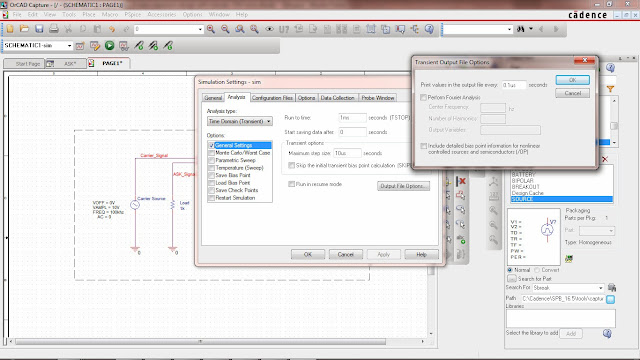
The simulation setting is shown in the figure below-
The output graph shown below shows the result of the simulation. The top graph is the binary message signal, the middle graph is the carrier signal waveform and the bottom graph is the ASK signal waveform.
Also see ASK Modulation Video Tutorial
Download ASK modulation simulation files:
http://www.filefactory.com/file/33tovaqoj98f/ASK_zip
For Phase modulation tutorial- see PSK modulation using orcad capture
In orcad capture a voltage controlled switch called Sbreak can be used to stimulate the behavior of the modulator. In reality a modulator is made of transistors that switches on/off in response to clock impulses supplied to it.
The schematic for simulating ASK modulation is shown in figure below-
 |
| Fig: ASK modulation schematic |
The simulation setting is shown in the figure below-
 |
| Fig: Simulation setting for ASK modulation |
The output graph shown below shows the result of the simulation. The top graph is the binary message signal, the middle graph is the carrier signal waveform and the bottom graph is the ASK signal waveform.
 |
| Fig: ASK modulation simulation output graph |
Download ASK modulation simulation files:
http://www.filefactory.com/file/33tovaqoj98f/ASK_zip
For Phase modulation tutorial- see PSK modulation using orcad capture
Tidak ada komentar:
Posting Komentar