This tutorial shows how to design a AMI Bipolar encoding circuit and simulate it using Orcad Capture and simulate the circuit to obtain the waveform. AMI(Alternative Mark Inversion) is a bipolar encoding technique that was and is still used in older PCM modems. The reason why it is useful is because if there is any bipolar violation then it is detected at the receiver and the error can be detected. The another reason is- because AMI is a bipolar RZ(Return to Zero) scheme it does not contain any DC component and therefore can used in telephony circuit where coupling transformers are used.
Circuit Schematic for AMI Bipolar Encoder
The circuit schematic of the AMI bipolar encoding circuit is shown below:
In the circuit, NRZ unipolar signal is generated using the SIM1 part from the source library. With SIM1 part we can generate a series of binary data with some defind bit period. In this example, a 7 binary bits "1011001" each of 100us(micro second) is generated and looped for 3 times.
The 7486 XOR gate, 7408 AND gate, 7401 AND gate, the transistors Q2N3906 and Q2N3904, the J-K flip flop 74107 are found in eval library. The diode D1N750 is found in the diode library. The rest are resistors, capacitors and voltage sources that are easily found.
After connecting the components as shown in the above figure, the AMI labelled wire is where the AMI bipolar signal appears.
Simulation
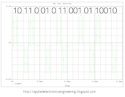
Create a new simulation profiel and set the simulation time for 2ms and run it. The resulting waveform is shown below-
Each bit duration is 100microsecond(100us) or 0.1 millisecond(0.1ms). From the waveform we can see that the 1 alternatives between +3V and -3V while 0 remains at 0V.
When clicking the FFT buttom on the probe we get the frequency spectrum of this RZ bipolar waveform as shown below-
From the spectrum figure 3, we can see that the AMI bipolar encoding has no DC component and thus is suitable for transmission over telephone lines and is useful for repeaters where ac coupling is required.
Also see baseband line code analysis blog post and NRZ Unipolar and NRZ Bipolar signal generation
Circuit Schematic for AMI Bipolar Encoder
The circuit schematic of the AMI bipolar encoding circuit is shown below:
 |
| Fig 1: AMI Bipolar Encoding Circuit Schematic |
In the circuit, NRZ unipolar signal is generated using the SIM1 part from the source library. With SIM1 part we can generate a series of binary data with some defind bit period. In this example, a 7 binary bits "1011001" each of 100us(micro second) is generated and looped for 3 times.
The 7486 XOR gate, 7408 AND gate, 7401 AND gate, the transistors Q2N3906 and Q2N3904, the J-K flip flop 74107 are found in eval library. The diode D1N750 is found in the diode library. The rest are resistors, capacitors and voltage sources that are easily found.
After connecting the components as shown in the above figure, the AMI labelled wire is where the AMI bipolar signal appears.
Simulation
Create a new simulation profiel and set the simulation time for 2ms and run it. The resulting waveform is shown below-
 |
| Fig 2: AMI Bipolar Encoding Pulse Waveform |
When clicking the FFT buttom on the probe we get the frequency spectrum of this RZ bipolar waveform as shown below-
 |
| Fig 3: AMI Bipolar Encoding with No DC component |
Also see baseband line code analysis blog post and NRZ Unipolar and NRZ Bipolar signal generation
Tidak ada komentar:
Posting Komentar