This article is about direct FM signal generation using varactor diode which illustrates how to design varactor FM modulator and explains the operation of varactor diode. The circuit diagram(schematic) and simulation was performed in orcad capture.
In a direct FM method of generating FM signal, the instantaneous frequency of the carrier signal is varied directly by the amplitude variation of message signal (generally called a modulating signal).
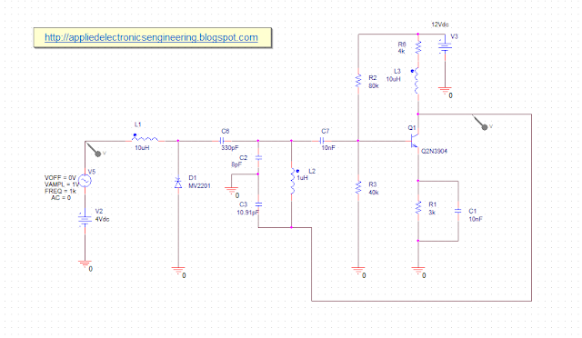
In the circuit diagram below, the message signal applied to changes the capacitance of the varactor diode MV2201 which in turn changes the frequency of the carrier signal oscillator. In effect, the variation of the amplitude of the message signal changes the frequency of the oscillating.
The message signal (stimulated as a single tone sine wave) varies the capacitance of the varactor diode MV2201. The varactor diode MV2201 which is forced into reverse bias operation by the DC supply of -4V along with the message signal is in parallel with the LC tank formed by the capacitors C1, C2 and the inductor L2. Hence the combination of the varactor MV2201, C1, C2 and L2 forms the LC tank (the feedback part) of the Colpitts oscillator of the carrier generating oscillator.
The resistors R1, R2, R3 and R6 forms the biasing elements for the transistor Q2N3904. This is the amplifying part of the Colpitts oscillator. The inductor L1 prevents the flow of RF signal generated by the oscillator from flowing back to the message signal generator. The capacitor C6 and C7 is a DC blocking capacitor. The capacitor C1 is a decoupling capacitor. The inductor L3 is the RF choke.
The picture below shows the message signal waveform-
The picture below shows the FM modulated signal waveform-
In the waveform above, a constant amplitude message signal was applied so that the output FM wave has a non-varying waveform.
In a direct FM method of generating FM signal, the instantaneous frequency of the carrier signal is varied directly by the amplitude variation of message signal (generally called a modulating signal).
In the circuit diagram below, the message signal applied to changes the capacitance of the varactor diode MV2201 which in turn changes the frequency of the carrier signal oscillator. In effect, the variation of the amplitude of the message signal changes the frequency of the oscillating.
 |
| Fig: Circuit Diagram of direct FM modulator using varactor diode |
The message signal (stimulated as a single tone sine wave) varies the capacitance of the varactor diode MV2201. The varactor diode MV2201 which is forced into reverse bias operation by the DC supply of -4V along with the message signal is in parallel with the LC tank formed by the capacitors C1, C2 and the inductor L2. Hence the combination of the varactor MV2201, C1, C2 and L2 forms the LC tank (the feedback part) of the Colpitts oscillator of the carrier generating oscillator.
The resistors R1, R2, R3 and R6 forms the biasing elements for the transistor Q2N3904. This is the amplifying part of the Colpitts oscillator. The inductor L1 prevents the flow of RF signal generated by the oscillator from flowing back to the message signal generator. The capacitor C6 and C7 is a DC blocking capacitor. The capacitor C1 is a decoupling capacitor. The inductor L3 is the RF choke.
The picture below shows the message signal waveform-
 |
| Fig: Sinusoid Message signal |
The picture below shows the FM modulated signal waveform-
 |
| Fig: FM modulated signal waveform |
Tidak ada komentar:
Posting Komentar